-

深圳市伟格兴电子科技有限公司
主营:集成电路销售,二三极管销售

深圳市伟格兴电子科技有限公司
主营:集成电路销售,二三极管销售 18
18

ttery Management IC For Li-Ion Powered Systems
1 Features The TPS65011 also has a highly integrated and
flexible Li-Ion linear charger and system power
1• Linear Charger Management for Single Li-Ion or management. It offers integrated USB-port and ACLi-Polymer
Cells adapter supply management with autonomous power-
• Dual Input Ports for Charging and From USB or source selection, power FET and current sensor, high
From Wall Plug, Handles 100-mA / 500-mA USB accuracy current and voltag
TLV和TPS一般会有pin to pin的对应型号;
一般来讲,TPS精度、准确度和性能会好一些,所以价钱要贵一些;
对应TLV就是一样可以实现上述功能,但是精度和性能等级是稍微低一点的;
具体选择原则,这个要看你的需求了,需要高性能就采用TPS,如果更看重成本可以选择TLV;
TPS的意思就是Ti Performance Solution, TLV 就是就是高性价比(Low Value)。
7.5 Electrical Characteristics
over operating junction temperature (TJ = –40°C to 125°C), typical values at VIN = 12 V and TA=25°C (unless otherwise noted)
PARAMETER TEST CONDITIONS MIN TYP MAX UNIT
SUPPLY
VIN Input voltage range(1) 3 17 V
IQ Operating quiescent current EN=High, IOUT = 0 mA,
device not switching
17 30
µA
TA = -40°C to +85°C 17 25
ISD Shutdown current(2) EN=Low
1.5 25
µA
TA = -40°C to +85°C 1.5 4
VUVLO Undervoltage lockout threshold
Falling Input Voltage (PWM mode operation) 2.6 2.7 2.8 V
Hysteresis 200 mV
TSD Thermal shutdown temperature 160
°C
Thermal shutdown hysteresis 20
CONTROL (EN, DEF, FSW, SS/TR, PG)
VH
High level input threshold voltage (EN,
DEF, FSW) 0.9 0.65 V
VL Low level input threshold voltage (EN,
DEF, FSW)
0.45 0.3 V
ILKG Input leakage current (EN, DEF, FSW) EN=VIN or GND; DEF, FSW=VOUT or GND 0.01 1 µA
VTH_PG Power good threshold voltage
Rising (%VOUT) 92% 95% 98%
Falling (%VOUT) 87% 90% 94%
VOL_PG Power good output low IPG=–2mA 0.07 0.3 V
ILKG_PG Input leakage current (PG) VPG=1.8V 1 400 nA
ISS/TR SS/TR pin source current 2.3 2.5 2.7 µA
POWER SWITCH
RDS(ON)
High-side MOSFET ON-resistance
VIN≥6V 90 170
mΩ
VIN=3V 120
Low-side MOSFET ON-resistance
VIN≥6V 40 70
mΩ
VIN=3V 50
ILIMF
High-side MOSFET forward current
limit(3)
VIN =12V, TA= 25°C
3.6 4.2 4.9 A
OUTPUT
ILKG_FB Input leakage current (FB) TPS62130, VFB=0.8V 1 100 nA
VOUT
Output voltage range (TPS62130) VIN ≥ VOUT 0.9 6.0 V
DEF (Output voltage programming) DEF=0 (GND) VOUT
DEF=1 (VOUT) VOUT+5%
Initial output voltage accuracy(4)
PWM mode operation, VIN ≥ VOUT +1V 785.6 800 814.4
mV PWM mode operation, VIN ≥ VOUT +1V,
TA = –10°C to 85°C
788.0 800 812.8
Power Save Mode operation, COUT=22µF 781.6 800 822.4
Tracking Feedback Voltage (TPS62130) VSS/TR = 350mV 212.6 225 237.4 mV
Load regulation(5) VIN=12V, VOUT=3.3V, PWM mode operation 0.05 %/A
Line regulation(5) 3V ≤ VIN ≤ 17V, VOUT=3.3V, IOUT= 1A, PWM
mode operation 0.02 %/V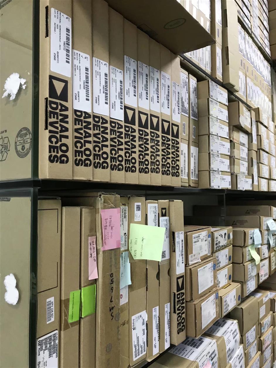
8-V to 14.7-V Input Voltage Range • Short-Circuit Protection
• V • Overvoltage Protection S Output Voltage Range up to 19 V
• TPS65161 has a 2.8-A Switch Current Limit • Thermal Shutdown
• TPS65161A has a 3.7-A Switch Current Limit • Available in HTSSOP-28 Package
• TPS65161B has a 3.7-A Switch Current Limit APPLICATIONS and 100-mA Charge Pump Output Current
• 1.5% Accurate 2.3-A Step-Down Converter • TFT LCD Displays for Monitor and LCD TV
• 500-kHz/750-kHz Fixed Switching Frequency
• Negative Charge Pump Driver for VGL
• Positive Charge Pump Driver for VGH
• Adjustable Sequencing for VGL, VGH
• Gate Drive Signal to Drive External MOSFET
DESCRIPTION
The TPS65161 family offers a compact power supply solution to provide all four voltages required by thin-film
transistor (TFT) LCD panels. With their high current capabilities, the devices are ideal for large screen monitor
panels and LCD TV applications.
ELECTRICAL CHARACTERISTICS (continued)
VIN = 12 V, SUP = VIN, EN1 = EN2 = VIN, VS = 15 V, V(LOGIC) = 3.3 V, TA = –40°C to 85°C, typical values are at TA = 25°C
(unless otherwise noted)
PARAMETER TEST CONDITIONS MIN TYP MAX UNIT
NEGATIVE CHARGE-PUMP VGL
VO Output voltage range –2 V
V(FBN) Feedback regulation voltage –36 0 36 mV
I(FBN) Feedback input bias current 10 100 nA
TPS65161, TPS65161A; IOUT = 20 mA 4.4
rDS(on) Q4 P-Channel switch rDS(on) Ω
TPS65161B; IOUT = 20 mA 3.7
I(DRN) = 50 mA, 0.13 0.19
TPS65161, V(FBN) = V(FBN)nominal –5%
TPS65161A I(DRN) = 100 mA, 0.27 0.42 V(FBN) = V(FBN)nominal –5%
V(DropN) Current sink voltage drop (3) V
I(DRN) = 100 mA, 0.24 0.42 V(FBN) = V(FBN)nominal –5%
TPS65161B
I(DRN) = 200 mA, 0.52 0.90 V(FBN) = V(FBN)nominal –5%
POSITIVE CHARGE-PUMP OUTPUT VGH
V(FBP) Feedback regulation voltage 1.187 1.213 1.238 V
I(FBP) Feedback input bias current 10 100 nA
rDS(on) Q3 N-Channel switch rDS(on) IOUT = 20 mA 1.1 Ω
I(DRP) = 50 mA, 0.40 0.68
TPS65161, V(FBP) = V(FBP)nominal –5%
TPS65161A I(DRP) = 100 mA, 0.85 1.60
Current source voltage drop V(FBP) = V(FBP)nominal –5%
V(DropP) V
(V(SUP) – V(DRP))
(4) I(DRP) = 100 mA, 0.63 1.60 V(FBP) = V(FBP)nominal –5%
TPS65161B
I(DRP) = 200 mA, 1.40 3.20 V(FBP) = V(FBP)nominal –5%
(3) The maximum charge-pump output current is typically half the drive current of the internal current source or current sink.
(4) The maximum charge-pump output current is typically half the drive current of the internal current source or current sink.
TPS62130, TPS62130A, TPS62131, TPS62132, TPS62133
5 Device Comparison Table
PART NUMBER OUTPUT VOLTAGE Power Good Logic Level (EN=Low)
TPS62130 adjustable High Impedance
TPS62130A adjustable Low
TPS62131 1.8 V High Impedance
TPS62132 3.3 V High Impedance
TPS62133 5.0 V High Impedance